GelSight – retrographic sensing capable for super-high-resolution 3D imaging
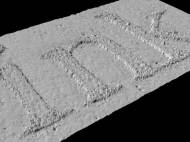 MIT researchers have combined a simple physical interface with computer-vision algorithms to create GelSight – a portable imaging system that can achieve resolutions previously possible only with large and expensive lab equipment. The device could provide manufacturers with a way to inspect products too large to fit under a microscope and it shows potential for applications in medicine, forensics and biometrics.
Unlike an earlier version of GelSight from 2009, which was sensitive enough to detect the raised ink patterns on a $20 bill, the new version of GelSight is capable to register physical features less than a micrometer in depth and about two micrometers across. It was developed by Edward Adelson, the John and Dorothy Wilson Professor of Vision Science at the Department of Brain and Cognitive Sciences and co-founder of GelSight, Inc., and Micah Kimo Johnson, who was a postdoc in Adelson’s lab at the time.
The system is less bulky and faster compared to confocal microscope or a white-light interferometer, which might take minutes or even hours to produce a 3D image. GelSight prototype sensor developed by researchers from researchers in MIT’s Department of Brain and Cognitive Sciences is about the size of a soda can, making it easily portable, and it can produce 3D images almost instantaneously. It also has a bench configuration version which is even more precise.
When GelSight system, which consists of a slab of transparent synthetic rubber with one side coated with a paint containing tiny flecks of metal, is pressed against the surface of an object the paint-coated side of the slab deforms. Multiple cameras mounted on the other side of the slab photograph the results, and computer-vision algorithms analyze the images of rubber’s deformation and produce 3-D models of an object. The result image can be manipulated on a computer screen for examination from multiple angles.
Although GelSight’s design is simple, it addresses a fundamental difficulty in 3D sensing – which is illustrated by the problem with a magnified photograph of an emery board, whose surface, in close-up, looks as a seemingly gelatinous combination of colors.
“The optical property of the material is making it very complicated to see the surface structure”, said Johnson, co-founder of GelSight, Inc. who previously helped develop the GelSight at MIT. “The light is interacting with the material. It’s going through it, because the crystals are transparent, but it’s also reflecting off of it.”
When a surface is pressed into the GelSight gel, the metallic paint conforms to its shape, and the optical properties of the surface become perfectly uniform and more readily visible. After applying some fairly standard computer-vision techniques, the acquired image is also easily.
A limitation of the system is that it can only capture shallow relief geometry. Although the sensor can be applied to any material, results gathered from surfaces with holes or fuzzy surfaces result with smoothed areas where the sensor fails to contact the subject.
GelSight system is complementary to current systems used to capture geometry such as laser range and structured light scanning. Designed in prototypes, it is already made for clients in aerospace, ballistics and metrology. It also shows a lot of potential for manufacturers of industrial equipment, dermatology and even biometrics.
For more information, you can read the paper presented at SIGGRAPH 2011 named: “Microgeometry Capture using an Elastomeric Sensor” (PDF).





Leave your response!