Metal oxide film transistor development breakthrough
 Researchers at the National Institute for Materials Science (NIMS) of Japan cooperated with researchers at the RIKEN Nanoscience Joint Laboratory to develop a metal oxide film transistor which utilizes a material with newly developed atomic composition. The new composition brings the use of potential amorphous silicon transistors successors in next-generation consumer displays a step closer to reality.
Current displays with amorphous silicon transistors are requiring increasing amount of power due to new high resolutions and touch panel features. Since there is only a little space left for improvement of the properties of the conventional material, new materials such as metal oxide film transistors are considered as an alternative to amorphous silicon thin films.
It has been found that metal oxide film transistors which are produced from a mixed target obtained by oxidizing indium, gallium, and zinc (IGZO film transistors), operate with high electron field effect mobility. However, IGZO film transistors also have a significant drawback since they require non-practical conditions where oxygen and moisture are being controlled.
While some research groups are searching for ways to develop techniques which allow control of thee factors, a team led by Dr. Kazuhito Tsukagoshi, a Principal Investigator at the NIMS International Center for Materials Nanoarchitectonics (MANA), succeeded in developing a different metal oxide material which could be suitable for use in new transistors.
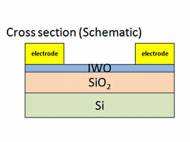
They came up with an indium-tungsten oxide (IWO) thin film by adding an extremely small amount of tungsten oxide to indium oxide. The developed material does not contain gallium or zinc, which are elements that are difficult to control in an amorphous state.
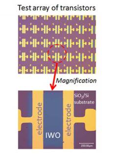
Because a homogeneous amorphous film can be produced simply by sputter film-forming at low energy, without heating the substrate or similar operations, thin films are easily formed with this new material, and operation as a transistor with high characteristics is possible, even using a structure without a protective film with an unprecedented thin film thickness of 10nm. Aside avoiding use of expensive gallium, the use of IWO thin film also reduces material costs since the total amount of raw materials used in the thin film is lower.
These new IWO film transistors could enable production of next-generation displays with higher resolution and lower consumption – a feature particularly important for displays in portable devices with power hungry displays. The technology developed by NIMS researchers could also be used for frequency improvement and resolution improvement in computer displays and televisions.


Leave your response!