Piezoelectric “taxels” enable human-like tactile sensing
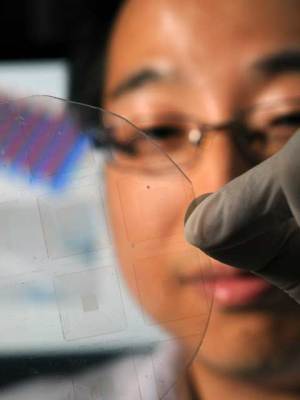
 Researchers at Georgia Insittute of Technology (Georgia Tech) developed arrays piezotronic transistors capable to convert mechanical motion into electronic signals. Named “taxels”, these touch-sensitive transistors could provide significant improvements in resolution, sensitivity and functionality for tactile sensing. The arrays could aid in robotics as tactile sensors, provide better security in handwritten signatures and offer new ways for information interaction.
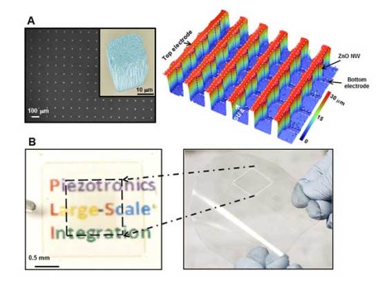
The researchers used bundles of vertical zinc oxide nanowires to fabricat arrays of piezotronic transistors. The arrays include more than 8,000 functioning piezotronic transistors, each of which can independently produce an electronic controlling signal when placed under mechanical strain. Their sensitivity is comparable to that of a human fingertip.
The devices developed by the Georgia Tech researchers rely on tiny polarization charges formed when piezoelectric materials such as zinc oxide are moved or placed under strain. In the piezotronic transistors, the piezoelectric charges control the flow of current through the wires just as gate voltages do in conventional three-terminal transistors.
The researchers used a chemical growth technique at approximately 85 to 90 degrees Celsius (185 to 194 degrees Fahrenheit), which allowed them to fabricate arrays of strain-gated vertical piezotronic transistors on substrates that are suitable for microelectronics applications. The transistors are made up of bundles of approximately 1,500 individual nanowires, each nanowire between 500 and 600 nanometers in diameter.
In the array devices, the active strain-gated vertical piezotronic transistors are sandwiched between top and bottom electrodes made of indium tin oxide aligned in orthogonal cross-bar configurations. A thin layer of gold is deposited between the top and bottom surfaces of the zinc oxide nanowires and the top and bottom electrodes, forming Schottky contacts. A thin layer of the polymer Parylene is then coated onto the device as a moisture and corrosion barrier.
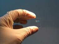
The array density is 234 pixels per inch, the resolution is better than 100 microns, and the sensors are capable of detecting pressure changes as low as 10 kilopascals – resolution comparable to that of the human fingertip. The transparency of arrays allows them to be used on touch-pads or other devices for fingerprinting. They are also flexible, foldable, and managed to operate after being immersed in both saline and distilled water for 24 hours.
The technology could be used for shape-adaptive sensing in which a change in the shape of the device is measured. In medicine, this technology could be useful in applications such as artificial/prosthetic skin or smart biomedical treatments where biological entities such as hair follicles or the hairs in the cochlea could be emulated. It could also be used for haptic feedback and intelligent robotics in which the arrays would sense what was in contact with them.
According to Zhong Lin Wang, a Regents’ professor and Hightower Chair in the School of Materials Science and Engineering at the Georgia Tech, future work will include producing the taxel arrays from single nanowires instead of bundles, and integrating the arrays onto CMOS silicon devices. Using single wires could improve the sensitivity of the arrays by at least three orders of magnitude.
For more information, read the article published in Science: “Taxel-Addressable Matrix of Vertical-Nanowire Piezotronic Transistors for Active/Adaptive Tactile Imaging” [5.67MB PDF]






Leave your response!